ARJ 2016, 0(1), P.P. 1-12;

					archives/2016/Rusul_Adnan/

					Research Article
Effect of Bias Voltage on Resonant Tunneling of Ga As/AlX
Ga1-X As Triple-Barriers Structure
Rusul Adnan Al-Wardy, Ph.D. Physics
Department of physics, College of Sciences, Wasit University, Kut, Iraq.
E-mail|:dr.rusuladnan|@|yahoo|.|com
Abstract
A theoretical study of resonant tunneling and current density of electrons
through Ga As/AlX Ga1-X As
triple-barriers system is presented within the energy range of electrons ε< the
potential barrier height (Vb). By use of the propagation
matrix method, the transmission coefficient of the structure is determined as a
function of the incident longitudinal electrons energy for different values of
applied voltage (Vs). Effect of well width and mole
fraction (x) of barrier are independently studied on quasibound
state energy with (ε < Vb), and also for resonant
tunneling current density for quasibound state. The solutions obtained are exact
and can be found easily by using MathCad program. Based on these calculations, a
new class of resonant tunneling superlattice devices can be designed.
Keywords: Ga As/AlX Ga1-X As
superlattice, transmission coefficient, resonance tunneling.
1. Introduction:
The single most useful quantum-confined structure in optoelectronics is arguably
the quantum well, which is a sandwich formed by thin layer of narrower-band gap
semiconductor trapped by two-wider band gap semiconductor layers. The periodic
structure containing a series of wells and barriers called "superlattice" (SL).
Fabrication of such structures was made by the molecular beam epitaxy (MBE) and
metal organic chemical vapor deposition (MOCVD) techniques [1]. The
coupling between wells in the (SL) causes the splitting in energy levels gives
rise to continuous bands known as (mini-band) which are separated by small
forbidden gaps [2]. When the special dimension is reduced to a scale that it is
comparable with the de Broglie wavelength of electrons, the wave nature of
electrons is expected to play in a very important role in tunneling properties
[3]. When electron incident on (SL) with effective mass (m*) and kinetic energy
(ε) is close to the eigen energy of the quantum well, this electron suffer
resonant tunneling and the transmission coefficient T(ε) is equal to one, i.e
the double barrier is totally transparent for particle transmission [2,4]. The
propagation matrix method (PMM) may be considered as one of the most accurate by
eminent researchers with this technique and the transmission coefficient can be
computed for double quantum-well triple-barrier heterostructure devices [5]-[9].
In this work, we report theoretical investigation on the transmission
coefficient and resonant tunneling current density through Ga As/AlX
Ga1-X As triple-barriers system under bias voltage.
Examining the dependence of transmission probability and the resonance tunneling
current density on a mole fraction (x), and the dimensions of well
width in the structure have been considered.
2. Theoretical Approach:
The triple-barrier system (TBS) is assumed to take the form of alternate
rectangular and wells at the conduction and valence band edges along the growth
direction. The low gap material, GaAs, forms the well, while the large gap
material, AlX Ga1-X As, forms
the barrier of the superlattice, as shown in fig. (1):-

Fig. 1 Band diagram of active region.
The one-dimensional, time-independent Schrödinger wave equation for an electron in a semiconductor heterostructure, under the envelope function/effective mass approximations is given as:
where x is the growing axis, εx is the
incoming electron energy, Ψ(x) is the wave function in the growing
direction and m* is the effective mass of each monolayer with potential energyV(x).
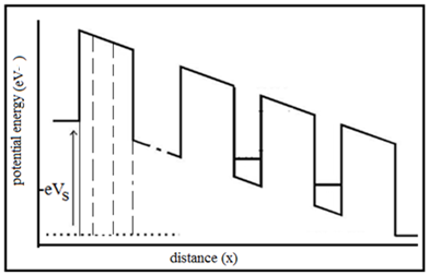
Fig. (2) represents the potential energy profile under an applied bias voltage
(Vs). We may neglect the valence band, as the holes are
much heavier than the electrons. The solutions of eq. (1) in each potential
region are given by the following equations:

Fig.2 the potential energy profile of conduction band under applied bias.
where Ai and Ci+1
are the coefficients for the wave functions traveling left to right in regions (i)
and (i+1) respectively, Di+1 and Biare
the corresponding right -to-left traveling wave's coefficients. The boundary
conditions are imposed between adjacent wave functions:
Substituting eqs. (2) and (3) into eq. (4) gave the following two equations:-
To solve the transmission probability, the Propagation-Matrix Method (PMM) used. One may writes eqs. (5) and (6) for potential step as a matrix equation [7,8]:-
Propagation between potential steps separated by distance (Si
= xi+1 -xi) carriers phase
information only so that:-
where
The propagation across the complete (i th) element consisting of a free propagation region and a step is:-
For the general case of (N) potential steps, the propagation matrix for each region and multiply out to obtain the total propagation matrix:-
Since the particle introduced from the left |A|2 = 1, and if there is no reflection at the far right then |D|2 = 0,
Once the transmission coefficient for longitudinal incident
electron energy under bias voltageT(εl,Vs
)can be obtained [9]:
Once the transmission probability is obtained, the current density through the structure is calculated using the Tsu-Esaki current formula [10]:
where εF is the Fermi energy(εF
= 0.005eV), T is the temperature (300K), εl is the
electron kinetic energy perpendicular to the device layers (in x-direction), kB
is the Boltzmann constant, and ma*
is the electron effective mass in GaAs. The tunneling electrons do not see any
potential change in the transverse directions and their transverse momentum
conserved. The electron longitudinal momentum (kx)
generally changes with distance [11].
3. Numerical Analysis:
We have calculated the numerical evaluation of transmission coefficient across Ga As/AlX
Ga1-X As triple-barrier system for incident energy(εl
< Vb), which is basic to found resonant
tunneling current density:
-
The barrier height at the conduction band edge is obtained from Dingle's rule assumed to be (88%) of difference between the band gaps of two materials GaAs, and AlXGa1-XAs [9,12]: Vb= 0.88(εgb - εga ). -
The energy band gap in the well (GaAs), εga = 1.428 eV, while the energy band gap in the barrier ( AlXGa1-XAs), is obtained from the formula:
εgb (x) = 1.424 + 1.247x (for x < 0.45). -
(x) = 5.6533 + 0.0078x.
The lattice constant of well material (GaAs) is aa -
The effective mass of the well material (GaAs) is ma* = 0.065m0, while the effective mass of barrier material ( AlXGa1-XAs) is obtained from the formula: mb* = 0.067 + 0.083x m0(for x < 0.45)[13].
4. Results and Discussions:
4.1 The Transmission Coefficient:
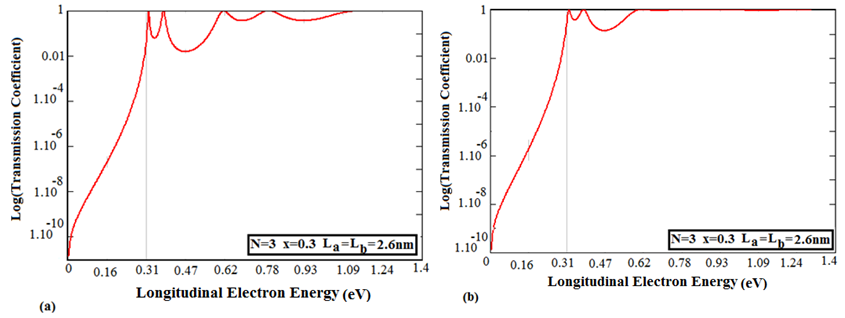
To study the transmission coefficient given by the resonant tunneling diode, we
have applied a bias voltage (Vs) in the top of the
emitter region. Figs. (3a-c) show the variation of Log (transmission
coefficient) as a function of incident longitudinal energy of electrons for
three barriers system (N=3), as a mole fraction (x = 0.3) and the dimensions of
the wells equal to barriers (La = Lb
= 2.6nm), and this for different applied bias voltage (Vs
= -0.27,0 and 0.31)V. The tunneling probability exhibit peaks when the
energy of the incoming electrons coincides with one of the quantized levels
inside the well, these electrons suffer resonant tunneling i.e. electrons tunnel
out without any significant attenuation in their intensity; these energies are
referred to resonant energies for (ε < Vb ), the first
peak from fig. (3) is referred to the ground state level (εo),
while the second peak is referred to the first excited state (ε1)[14].
When the applied bias voltage is increased, the transmission probability slowly
deceases down to small electron energy values, i.e. all the resonant peaks of
transmission probability become hidden, mainly due to the slope of the barrier
potential .This behavior has also been reported in similar structures by C.
E.Simion et al [7] and R. Djelti et al [15].


Fig. 3 Log (Transmission coefficient) versus longitudinal
electron energy for GaAs/ AlX Ga1-X
As at (a) Vs= -0.27V, (b) Vs =
0V, (c) Vs = 0.31V.
4.2The Resonance Tunneling Energy:

Figs. (4a, b) shows the relationship between the ground state
levels (ε0) in the quantum well as a function of the
bias voltage (Vs) for (GaAs/AlX
Ga1-X As) triple-barrier structure. It is so clear, from
these figures that the ground state level decreases as we increase the bias
voltage, this is due to the confinement of the states in the miniband which
become increasingly important [16, 17]. Also, it is clear from figure (4a) that
high mole fraction of (Al) in the system, give a higher level value since we are
dealing with low energy gap. While figure (4b) shows the increasing of the well
dimension, resonant tunneling phenomenon is evident at lower energy values [8,
14], that is because from the law of the energy levels in the quantum well,
energy levels inversely proportional to the square of the well width and this
law explain this behavior of the levels shifting when reduced or increased in
well width and move higher or lower energy values, respectively.
Fig 4. Dependence of ground state level on bias voltage for
GaAs/AlX Ga1-X As.
4.3The Resonance Tunneling Current Density:
The current density (at room temperature , εF
= 0.005eV) is derived by integrated the transmission coefficient T(εl,
Vs ) over all relevant states in the basis of eq. (17).
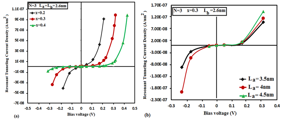
Figure (5) depicts the resonant tunneling current density for ground state level
(J0) as a function of bias voltage (Vs) for
(GaAs/AlX Ga1-X As) superlattice
structure. The net tunneling current, at zero applied voltage, is zero, because
the Fermi-level is constant across the junction and no filled states exist
(electrons) on either side of the junction, while below the Fermi-level there
are no empty states available on either side of the junction. Physically, when a
bias voltage applied to the structure a small current flow such that the
resonant energies (εo state) approach the Fermi energy of the
electrons at the left of the barrier. The current density increases strongly as
voltage increase, when the energy of the incident electron coincides with the
energy of one of confined states. Further increase of the bias voltage (Vs
> potential barrier height Vb)detunes all the resonant peaks of
transmission probability become hidden that is result no resonant tunneling
current density, this result also has been reported by A. Zarifkar et al
[6]. From in figure (5a) noticed that when increasing the mole fraction of (Al)
content, the resonant tunneling current density for ground state level (J0)
will decrease. This behavior comes in agreement with the results in experiment
by others S. Mukherjee et al [17], M. Tsuchiya et al [18] and
H.Sakaki et al [19]. The explanation of this behavior is expected when
increasing the mole fraction of (Al), (x = 0.2,0.3 and 0.4), it which will cause
an increase in the barrier height, (Vb = 0.21,0.32 and 0.43) eV,
respectively. That is due to poor tunneling through barriers, because the
necessary conditions for tunneling occur when potential barrier height is low
and the transmission coefficient will be decrease so (J0)
will decrease, as in eq. (17). While fig. (5b), presented that when increasing
of well width, the resonant tunneling current density for ground state level (J0)
will increase, this that make agreement with author R. Djelti et al [15].
It should be pointed out that the band gap between miniband become decrease due
to continuous energy state and the quantum confinement effect will be decrease.
The electron mobility increases and drift velocity will be increase (J = nevd).

Fig 5. The (J0 - VS)
curve for GaAs/ AlX Ga1-X As (a)
at x=0.2,0.3 and 0.4(b) at well width (3.5,4 and 4.5)nm and constant barrier
width=2.6nm.
From these results, we can put relationship between resonant tunneling current density and the energy levels in the structure, as shown in fig. (6), at high energy levels, the resonant tunneling current density will be decrease that is related with quantum confinement effect.

Fig. (6): Dependence the resonant tunneling current density on energy levels.
5. Conclusions:
We have numerically determined the effect of each of bias voltage, mole fraction
of (Al) and well dimension on the transmission coefficient, resonant tunneling
energy and the resonant tunneling current density for ground state level of
GaAs/ AlX Ga1-X As triple-
barrier structures. We can conclude that by propagation matrix method which is
simple and accurate method to determine transmission probability as result to
find current density (for ε < high of barrierVb). Under high voltage
bias it will in generally be much harder to obtain resonant tunneling, mainly
due to low energy level and high current density. In addition, high value of
mole fraction gives high energy level for ground state level but low current
density because of potential high barrier increasing. While high well width one
will find low energy level but high resonant tunneling current density.
Acknowledgment
We are grateful to Dr. Moafac C. Abdulrida (Nanoscience Laser and Devices Group) for his fruitful discussion.
References
[1] J.D.Cressler, "Silicon Heterostructure Devices" CRC press, Taylor and
Francis group, (2008).
[2] S.M.Sze and K.K.Ng, "Physics of Semiconductor Devices", 3rd edition, John
Wiley & Sons., Inc. (2007).
[3] X.W.Liu and A.P.Stamp, "Resonant Tunneling and Resonance Splitting: The
Inherent Properties of Superlattices", Physical Review B50, no.3, (1994).
[4] S.P.Bhattacharya and S.Sinha, "Non-Relativistic Formalism of Resonant
Tunneling in The Semiconductor Superlattices", Journal of Physical Science,
Vol.12, (2008).
[5] A.F.J.Levi, "Applied Quantum Mechanics", University of Southern California,
A.Levie, P.111-125, (2003).
[6] A.Zarifkar, A.M.Bagherabadi, "Numerical Analysis of Triple-Barrier GaAs/AlxGa1-xAs
Resonant Tunneling Structure using PMM Approach", IJCSNS International Journal
of Computer Science and Network Security, Vol.8, No.6, P.266-270, (2008).
[7] C. E.Simion, C. I. Ciucu, "Triple -Barrier Resonant Tunneling: a Transfer
Matrix Approach", Romanian Reports in Physics, Vol. 59, No. 3, P. 805-817,
(2007).
[8] R. Karmakar et al, " Calculating Transmission Coefficient of Double Quantum
Well Triple Barrier Structure having Parabolic Geometry using Propagation Matrix
Method", International Journal of Engineering and Advanced Technology (IJEAT)
ISSN: 2249 - 8958, Volume-1, Issue-2, December (2011). (e-mail: rajit.karmakar@gamil.com).
[9] J.Nanda et al, "Transmission Coefficient, Resonant Tunneling Lifetime and
Traversal time in Multibarrier Semiconductor Heterostructure", Physika B, 383,
P.232-242, (2006).
[10] R.Tsu and L.Esaki, "Tunneling in a Finite Superlattice", Appl. Phys. Lett.
Vol.22, No.11, P.562-564, (1973).
[11] J.P.Sun and G.I.Haddad, "Resonant Tunneling Diodes: Models and Properties",
Proceedings of the IEEE, Vol.86, No.9, P.641-661, (1998).
[12] M. Tsuchiya and H. Sakaki, "Dependence of Resonant Tunneling Current on Al
mole fractions in Alx Ga1-x As
GaAsAlx Ga1-x As Double Barrier
Structures", Appl. Phys. Lett. 50, 1503, (1987).
[13]
http://www.ioffe.ru/sav/NSN/semicond/AlGaAs/index.html, Jun, (2013).
[14] S. A. Almansour, D. Hassen, "Theoretical Study of Electronic Transmission
in Resonant Tunneling DiodesBased on GaAs/AlGaAs Double Barriers under Bias
Voltage", Optics and Photonics Journal, 4, 39-45, (2014). (e-mail:h dakhlaoui@yahoo.fr).
[15] R. Djelti et al, "Resonant Tunneling in GaAs/AlxGa1-xAs Superlattices with
a Periodic Potential Profiles", Superlattices and Microstructures 50, p.
659-666, (2011). (E-mail address:djeltired@yahoo.fr (R. Djelti).
[16] Z. Aziz et al, "Suppression of The Singularly Localized States in Dimer
Quasiperiodic Fibonacci Superlattices", Solid State Communications 150, P.
865-869, (2010).
[17] S. Mukherjee et al, "Theoretical Computation of Transmission Coefficient of
Double Quantum W ell Triple Barrier Structure in Presence of Electric Field",
International Journal of Soft Computing and Engineering (IJSCE) ISSN: 2231-2307,
Volume-1, Issue-NCRAMT2011, July (2011).
[18] M. Tsuchiya, H. Sakaki, "Dependence of Resonant Tunneling Current on Well
Widths in ALAs/GaAs/ AlAs Double Barrier diode Structures", Appl. Phys. Lett.
49, 88, (1986).
[19] H.Sakaki et al, "Resonant Tunneling in Quantum Heterostructure: Electron
Transport, Dynamics, and Device Applications", IEEE Journal of Quantum
Electronics. Vol. 25. No. 12, (1989).
© 2016 by the authors; licensee ARJ